Electron Beam Lithography

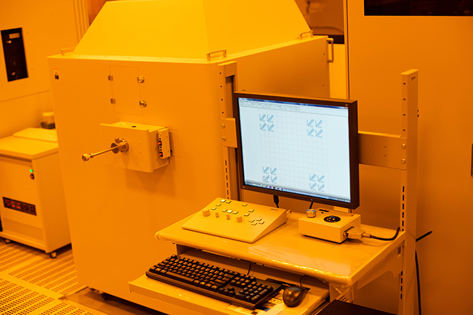
EBL CRESTEC CABL AP50E/RD
The CABL-AP50E/RD Electron Beam Lithography system is designed for high-resolution applications in academic research and development. It supports multiple scanning modes, including vector and raster, for precise and flexible pattern creation. The system has advanced stitching capabilities and a stable environment control system.
Acceleration voltage
50kV
Minimum beam diameter
2nm
Sample size
Up to 150mm

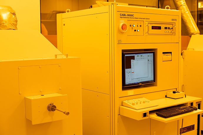
EBL CRESTEC CABL-9510C
This Electron Beam Lithography system employs both vector and raster scanning techniques, where the electron beam follows specific patterns to define intricate structures on a substrate. The Gaussian-distributed electron beam ensures a focused and precise energy distribution, allowing for highly accurate and fine resolution patterning
Acceleration voltage
50kV
Minimum beam diameter
2nm
Sample size
Up to 150mm

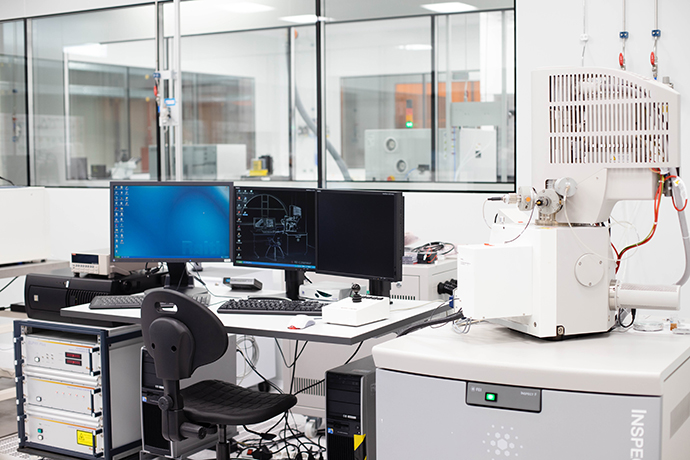
SEM FEI InspectF50 + EBL Raith Elphy Plus attachment
The FEI Inspect F50 SEM is a high-resolution scanning electron microscope designed for advanced imaging and analysis of materials at the nanoscale. When equipped with the Raith Elphy Plus attachment and laser interferometric stage, it enhances its capabilities for Electron Beam Lithography (EBL), allowing for precise patterning and fabrication of micro and nanoscale structures.
Acceleration voltage
1-30kV
SEM resolution
1.2nm at 30kV
Sample size
Up to 50mm