Electron and Ion microscopy

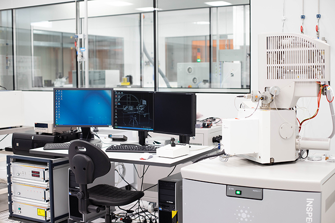
Scanning Electron Microscope Zeiss Gemini 560
The Gemini 560 SEM, from Zeiss, is a field emission scanning electron microscope. This instrument combines excellent low-voltage performance, high-resolution sub-nanometer imaging, and integrated analysis capabilities.
Acceleration voltage
0.02–30 kV
Resolution
≤ 1 nm at low KV (0.8 nm @ 1 kV, 0.5 nm @ 15 kV)
Electrons detectors
Everhart Thornley In-chamber Secondary Electron Detector, In-Column Secondary Electron Detector, In-Column Backscattered Electron Detector with Energy selection filter, Variable Pressure Secondary electron Detector (VPSE)
Imaging Modes
High Vacuum mode (standard), Variable Pressure at lower vacuum for imaging non-conductive specimens without additional anticharging preparation, and enhanced Variable Pressure mode inserting a Beamsleeve aperture below the objective lens.
Analytical detectors
EDS and EBSD (see corresponding section)

Focused Ion Beam Zeiss Orion Nanofab
The Zeiss Orion Nanofab is a multi-ion beam platform that combines helium and neon gas ion sources for ultra-high-resolution imaging, nanomachining, and nanofabrication. He ion beam is used for sub nanometer imaging with great surface sensitivity and large depth of field and for nanofabrication for ultra-high resolution patterning. Neon ion beam is used for nanofabrication of larger structures thanks to stronger sputtering yield than helium.
Resolution
He ion beam 0.5 nm, and Ne ion beam 1.9 nm
Beam energy
10 keV-30 keV (He), 500eV-30 keV (Neon)
Sample transfer
loadlock with max sample size 100 mm
Electrons detectors
Everhart Thornley In-chamber Secondary Electron Detector
Imaging Modes
High Vacuum mode (standard) and charge compensation by electron flooding on the sample surface.
Patterning capability
Add-on to perform nanolithography by controlling beam position and blanking by FIBICS NPVE software.

Focused Ion Beam / Scanning Electron Microscope Zeiss Auriga Crossbeam
The Zeiss Auriga Crossbeam is a dual-beam FIB-SEM system that combines a field emission Scanning electron microscope (SEM) with a focused Ga⁺ ion beam (FIB), enabling high-resolution imaging and precise nanofabrication or cross-sectioning.
Resolution
SEM 2.5 nm @ 1 kV, 1 nm @ 15 kV; Ga ion beam 5 nm @ 30 kV
Beam energy
100 eV-30 keV (SEM), 500eV-30 keV (Ga)
FIB current
1 pA –20 nA
Sample transfer
loadlock with max sample size 100 mm.
Electrons detectors
Everhart Thornley In-chamber Secondary Electron Detector, In-Column Secondary Electron Detector, In-Column Backscattered Electron Detector with Energy selection filter
Imaging Modes
High Vacuum mode (standard) and charge compensation by nitrogen gas flooding on the sample surface.
Patterning capability
add-on to perform nanolithography by controlling beam position and blanking, to perform large area mapping and to do 3D FIB SEM tomography by FIBICS Atlas5 software. Gas injection system to deposit locally Pt (to protect the sample surface before ion milling) or to etch locally by XeF2 or water precursors.